Introduction
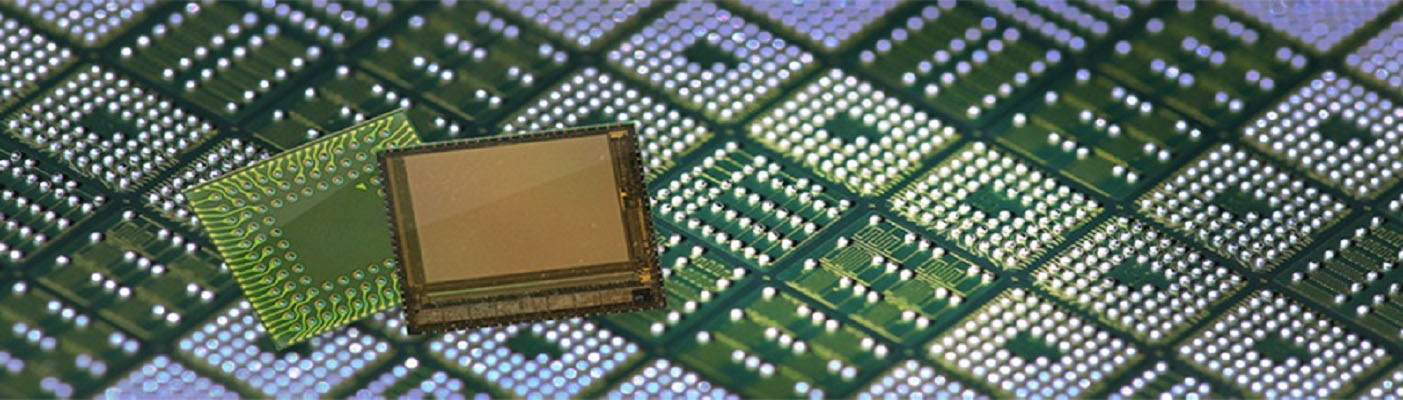
Xintec was the first package house which commercialized wafer level chip scale packaging (WLCSP). Started from Wafer Level CMOS image sensor packages, Xintec has expanded services across various sensor package services over optical, MEMS and customized wafer lever structure which can be utilized in consumer, communication, computer, industrial and automotive categories.
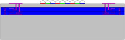
Optical sensor service offering
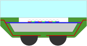
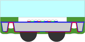
- Chip Scale Package (CSP), we offer
- Two type of RDL interconnect: Side-wall interconnect (XinPac) & Through Silicon Via (XinTSV).
- Various glass thickness and filters such as double AR, IR/AR…etc.
- Glass bonding to wafer with or without cavity.
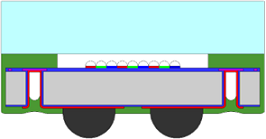
- Wafer Reconstruction (RW)
- We offer FSI/BSI/Stack wafer reconstruction for mobile, automotive, consumer applications.
- Specialty RW service: XinLid-a-G
- We offer RW with Glass Lid for Automotive application, which protect wafers against particles in subsequent assembly processes.
Xintec Service: Optical Sensor
| CIS | NIR/ALS/DOE | |||
|---|---|---|---|---|
| Automotive | Mobile | Industrial / Medical | Mobile / Watch / ARVR | |
| VGA >2M | 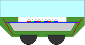 XinPac-a-G |
 XinPac-G |
 XinTSV-1-G |
 XinPac-OP |
| >8M & >48M |  XinLid-a-G>=8M  |
 Stacking CIS R.W.>=48M  |
 XinTSV-3-G  |
 XinTSV-3-OP  XinPac-D  |