客製化服務介紹
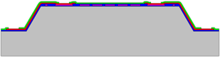
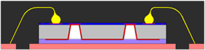
- 3D I/O 重佈線
- 降低焊墊層高度,使感測器能與平整表面無縫貼合。
- 電源與接地強化
- 利用矽穿孔技術連接接地焊墊與背面電鍍銅,以達成散熱與降低雜訊之需 求。
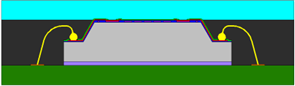
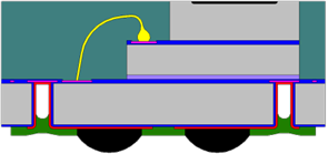
- 雙面連接技術
- 在晶圓表面提供鎳鈀金(Ni/Pd/Au )或銅柱,搭配矽穿孔技術連接頂部晶片與底部載板。
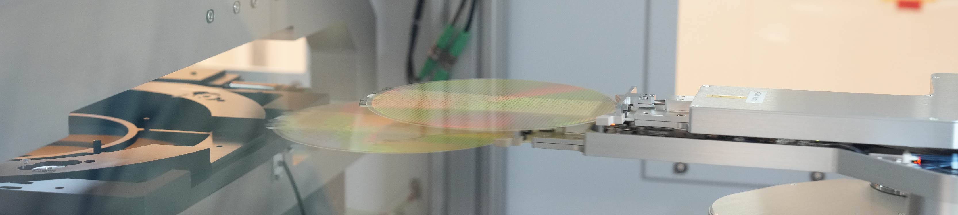
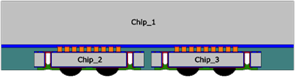
精材科技技術方案: 客製化技術
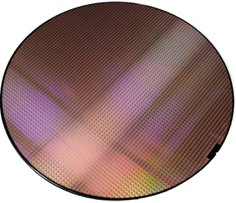
| 晶圓進件 | 晶圓處理製程 | 元件封裝 | 終端應用 | |
|---|---|---|---|---|
| 3D I/O 重佈線 |
 |
 XinPPI-M |
|

|
| 電源接地強化 |  XinTSVG |
 QFN |
|
|
| 雙面連接 | 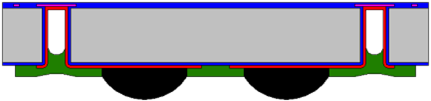 Lidless-TSV  Duo-C |
  |

|